Faculty of mechanic
University of Maribor
Rules
Only words with 2 or more characters are accepted
Max 200 chars total
Space is used to split words, "" can be used to search for a whole string (not indexed search then)
AND, OR and NOT are prefix words, overruling the default operator
+/|/- equals AND, OR and NOT as operators.
All search words are converted to lowercase.
FEI Sirion 400 NC
High-resolution scanning electron microscope with field electron emission, which enables extremely high magnifications (up to a million times) and high resolution (1 nm).
It is equipped with an EDS (Energy Dispersive Spectroscopy) analyzer, Oxford Instruments.
It has a Schottky electron source, where a field emission produces a beam of electrons with a small diameter and a high density.
The result is high resolution, even at low voltages:
- 1.0 nm at 15 kV
- 2.0 nm at 1 kV
This is the main feature and the biggest advantage of this microscope.
Due to the good resolution at low voltage, in addition to conductive materials, non-conductive samples and materials with a small atomic number can be observed in high vacuum or low vacuum (up to 130 Pa).
The microscope is equipped with a detector for secondary (topographic contrast) and backscattered electrons (topographic and Z-contrast).
It is intended for the characterization of conductive and non-conductive samples.
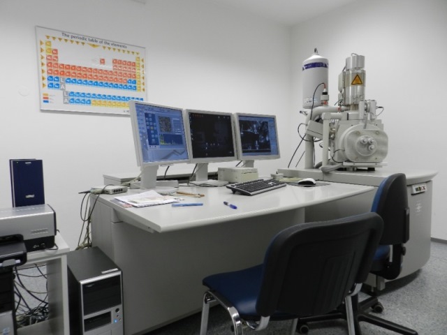
Technical information
Schottky electron source that allows for a resolution of;
- 1.0 nm at 15 kV;
- 2.0 nm at 1 kV;
- accelerating voltage from 200 V to 30 kV;
- magnifications from 30 x to 1 000 000 x;
- five motorized axes (x = 100 mm, y = 100 mm, z = 60 mm, tilt (-15 to 75 degrees) and rotation (n x 360 degrees));
- the size of the chamber equipped with an infrared camera is 379 mm from left to right.
INCA 350 (EDX-analyzer)
The microscope is equipped for microchemical analysis with an energy dispersion spectrometer EDS Oxford INCA 350.
It enables qualitative and quantitative microchemical analysis in a single point and on the surface, as well as qualitative line analysis and surface distribution of elements (mapping analysis).
Elements from beryllium to uranium can be analyzed.
Basic technical characteristics:
- the resolution of the EDS detector is 129 at Mn Kα