Rules
Only words with 2 or more characters are accepted
Max 200 chars total
Space is used to split words, "" can be used to search for a whole string (not indexed search then)
AND, OR and NOT are prefix words, overruling the default operator
+/|/- equals AND, OR and NOT as operators.
All search words are converted to lowercase.
Scanning electron microscopy - SEM
At UCEM, we use two scanning electron microscopes for different samples:
Type of sample | Conductive | Non-Conductive | Damp | Dirty, greasy | Resolution |
+ | + | + | + | 3,5 nm at 30 kV (high vacuum) 3,5 nm at 30 kV (ESEM mode) 15 nm at 3 kV (low vacuum) | |
+ | + | - | - | 1,0 nm at 15 kV 2,0 nm at 1 kV |
Examples of scanning electron microscopy:
Characterization of materials with FIB/SEM
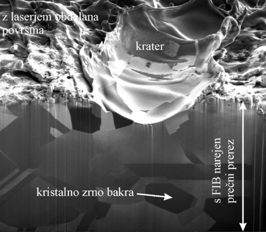
Characterization of materials with FIB/SEM (focused ion beam on a scanning electron microscope) is one of the most advanced methods for materials analysis. It allows simultaneous physical processing of materials with a focused beam and photographing the exposed surfaces of the samples below the surface. The method was used in the latest study (2015) of laser-treated surfaces and published in one of the most prestigious journals in the field of materials surface research: Applied Surface Science; Damage caused by a nanosecond UV laser on a heated copper surface, V. Henč-Bartolić , T. Bončina, S. Jakovljević, P. Panjan, F. Zupanič. Reputable researchers from UM FS, IJS and the University of Zagreb were included in the research.
Development of cell cultures
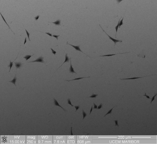
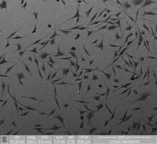
With the above equipment, it is also possible to characterize the development of various cell cultures that grow on the contact surfaces of biomaterials. L929 cells shown under the same conditions on two different surfaces are shown: a) on a polished NiTi alloy or b) on a surface of plasma-treated NiTi alloy.
Measurement of layer thickness on different samples
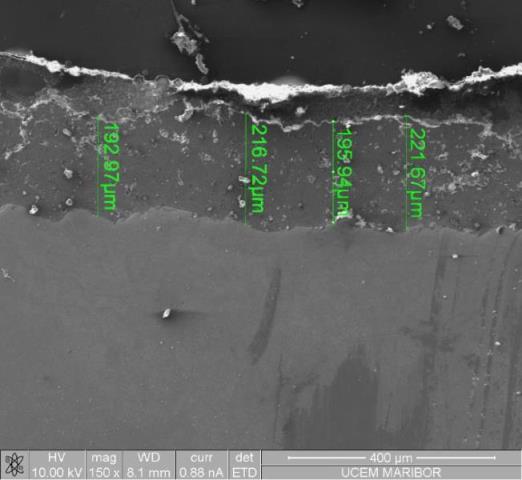
Other examples of using the SEM: roughness measurements, study of the fracture surfaces of metals, characterization of materials, corrosion measurements, dimensional measurementss at nanometer size, etc.
Characterization of materials with STEM detector
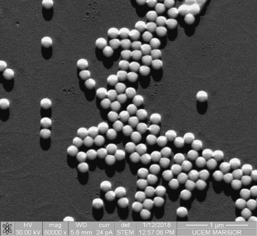
Scanning transmission electron microscopy (STEM) is the ability of a microscope to combine the principles used in transmission electron microscopes (TEM) and scanning electron microscopes (SEM). STEM is a popular technique for laboratories without a transmission electron microscope (TEM). STEM detectors extend the imaging capabilities and analytical power of the SEM and FIB-SEM systems by obtaining unique information obtained with transmission electrons. Samples analyzed by this technique must be prepared in the form of thin lamellae <100 nm thick. This technique can be used in combination with elemental analysis, such as EDX and EBSD, for microanalysis of samples at high resolution.
The transmission electrons scattered through the sample at different angles give different data from the sample. The following signals are available:
- The Bright Field (BF) signal represents the typical contrast of the Bragg diffraction orientation and the absorption contrast in the lamellae.
- Dark Field (DF) contains partial orientation contrast and material contrast of light elements.
- The High Angle Dark Field (HADF) contains the highest material contrast with the lowest Bragg diffraction contrast.
The scattering angles depend on the sample material, the lamella thickness, and the electron beam energy. The STEM detector enables the investigation of structure in biological samples, analysis of faults in semiconductor devices and characterization of materials.
The microscopes on the UCEM enable the connection of a STEM detector, which enables us to observe the characteristics at the nanometer level.

